 |
Romano Cartoceti, I4FAF
Sergio Cartoceti,
IK4AUY
Roberto Danieli,
IK4AVZ
| This article has been originally published
(we completed it in May 1999) in ARI Magazine Radio Rivista in April 2000,
pages 23-29. From Radio Rivista on line service 02/2010: click here to down load the original article Last text update: 06 Jan 2004; last errata corrige update: Feb 2010. Component value ERRATA CORRIGE: trimmer R28, in bias regulator, must be 10 Kohm for high voltage mosfets (and not 1 Kohm). Ampli schematic has wrong value 4.7KOhm for R11,R12,R13,R14: good one is in components list= 4,7 Ohm, 1/2 W. T3 in PDF file document C. output transformer uses FT-50-43 (and NOT the smaller FT-37-43). |
|
1. HF QRP Linear Amplifier 2. Circuit description 3. Practical work and bias regulation 4. Tests and performances 5. Mosfets Vs Transistors IMD 6. Mosfets Linear Ampl components list 7. Bias regulator components list 8. Bibliography and notes |
Click
below here to download zipped (pdf) files, then unzip and print with Acrobat Reader at 100% size. A. Schematic diagram Mosfets bias regulator B. Schematic diagram low cost Mosfets QRP HF Lin Amp C. RF Transformer details for push pull QRP Mosfets D. Mosfets to Heat Sink mounting details E. Low Cost Mosfets HF QRP pcb top side F. Low Cost Mosfets HF QRP, pcb mirrored bottom side G. Low Cost Mosfets HF QRP, components placement H. Output Low Pass filters for Amateur Bands (link to CDG2000 fine project + fwd, rev directional coupler) |
Optimised QRP Low Cost Mosfets HF Linear
Amplifier with low IMD
Max safe output power is around
10 to 15 watts pep or CW with good IMD, but be careful to dissipation and heat
so I suggest a large metallic heat sink cooler and an air blower (fan).
Disclaimer: we are not responsible for any damage or use of any kind you
do or could arise in anyway with this material here presented.
|
|
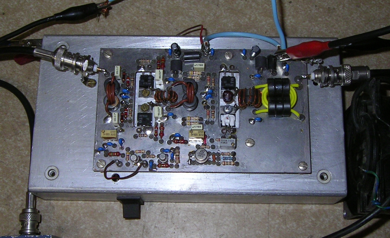
CLICK HERE
FOR assembled unit PHOTO
HF QRP Linear Amplifier with low cost Mosfets (here is a brief translation)
Our main goal was to get an optimized low cost Mosfets Linear Amplifier
circuit for QRP, with around 10 - 15 Watts PEP or CW average power for SSB and
CW, with lower higher order IMD in the 1.8 to 30 Mhz, for
Amateur Radio use, to compare it with a similar circuit adapted around plastic
case transistors with a 13.8 V power supply, both with variable bias capability, to improve home base station
performances, where it is easily possible to get other than 13.8 V power supply
for TX finals.
This Mosfet unit operates at 28 V and the high bias current used requires a
large Heat Sink and air blower (fan) always on while in TX to mantain these
plastic devices well below their maximum power dissipation and temperature
limits inside a SOA safe
operating area point of work. We used low cost Mosfets devices that ended to
show us good RF performances, but you could also change the project to try
specifically rated RF Mosfets, of course with some minor mods if eventually
required, for even lower IMD performances, with more rugged ceramic case
like the MRF series, but at much higher prices, already seen in some
high level commercial amateur radio transceivers (1). In general
linearity at RF is seen as a) uniform gain - frequency relation;
b) low intermodulation IMD as monitored with a two tone test (at a small
frequency separation around 1 to 2 Khz or if not otherwise possible at a
larger separation) with a well regulated power supply for the unit. This is
of course an approximate "best case" SSB performance
test any way since in SSB voice is a whole band of audio frequencies not only
two (agree with W8JI Tom advices, see TOPBAND reflector); c) attenuation of harmonic frequencies (the higher level is in the odd
multiple of fundamental output frequency but the closer one is the second and it
must be adequately filtered with output low pass filters to get values below -
40 dB down as per FCC or other national laws. Of course in b) and c) the higher
the attenuation the better is (dB with minus sign).
We and other amateurs (3) wanted to test these low cost fast switching Mosfets
that you can find very easily.
Some advantages that mosfets have over transistors (4): higher gate impedence to
DC make easier to implement a bias circuit without DC current power transistors
in the bias circuit and mosfets behaves better, at raising temperature of work,
with a self protection action because there is a lowering in the drain-source
current; an higher output impedence together with an higher DC power supply make
easier to project and built the output RF transformer; the IRF510 is
easy to get and inexpensive
(5). In the negative side Mosfets are sensitive to electrostatic discharges and
it is commonly guessed that they could self-oscillate
(more than transistors) but in all tests we have performed around this
circuit and our pcb layout it did not happen.
Of course with a 28 V power supply it is not intended for portable
operation. We think that the worst of the previously negative
aspects is a lower efficiency: to get a better linearity (lower IMD) we need to
set the point of work near class A so we have higher quiescent currents while in
TX . The high (stable) gain achieved with 2 stages (2x
IRF510 + 2x IRF510) with a lower higher IMD order performances (that means lower
splatters if you drive another linear amplifier to get an higher output level)
and these devices are so easy to get and low priced that it is interesting to
give them a try.
This circuit is a broadband one from 1.8 to 30 MHz, so it is "no-tune" and you need only to regulate the quiescent current bias multiturn trimmer of each Mosfets couple. This means also low efficiency (for a lower IMD it is even low as around 20-30%) together with good heat sink + blower system. The push-pull configuration permits to get a better attenuation of even harmonic frequencies (a good benefit since the second is the closer 2x fundamental freq.). The output stages have 2 separate transformers in each couples so the power supply current does not flow in to the output transformer to avoid saturation and the floating winding helps for balance for harmonic attenuation and stability (6). We have emploied also in this low power unit the circuit found in higher power units to stabilise thermically and regulate the bias current around a trusted LM723 IC (7) , the transistors are used only for PTT control. In the first stage Mosfet couple we have used a feedback circuit to optimize gain-frequency response (8). Without it the low frequency gain is very high, too high: at 3 MHz 50 dB ! and a lower 30 dB at 30 MHz, but with this feedback circuit the overall gain variation is close to a +/-3 dB, a good result. We tried a similar feedback in the output couple but results where a poorer IMD performance so it has been omitted. We selected Mosfets couples in a simplified way (while not so precise RF matching practice) measuring drain-source resistence: a better way could be to measure in a simple test circuit current drain at a given gate voltage applied for all devices and choose the ones that showed closer current values.
Practical work and bias regulation
The pcb board is a 14x9 cm. double sided epoxy glass, through holes should be soldered for a better ground plane, the top side is unetched to form a ground plane, and carry all the components except the power Mosfets that are mounted sitting inside the pcb holes and insulated with mica (apply a silicon grease to enhance warm dissipation) to the heat sink plane (see detailed drawing), the leads are soldered directly on the tracks to give a low inductance connection. Pay attention to electric isolation of the Mosfets since their metallic portion is internally connected to Drain (9). The RF transformers are made easily with two rows of 3 toroidal ferrites without a mechanical support but with some glue and we have used teflon insulated (thin) wire with a larger possible diameter (10). The first 2 transformers are vertically mounted to save space and avoid unwanted couplings (11). Check everything for unwanted short circuits and without RF signal and before applying DC Voltage regulate both trimmer bias for minimum voltage to the gates. Connect V dc to first couple and regulate the bias with the multiturn trimmer R29 for a quiescent bias current, no RF, around 500 mA (total first couple bias), then regulate the bias of the output second couple for about 1 A (total second couple bias) with multiturn trimmer R30. The trimmer that control the thermistor action, R28, should be regulated while warming up mosfets and alternatively lowering temperature and it should be regulated so that the bias currents change only a little to the difference in temperature (you should do it again a few times). At this point you can connect a wattmeter at the output to a 50 Ohm dummy load and check amplification that should be close to our data in table (A). Pay attention that since this is a broadband amplifier you must lower output harmonic frequencies well below at least 40 dB as required by laws (FCC or national regulatories) so you need lowpass filters well matched to the output impedence of this unit and 50 Ohm antenna impedence. Remember that a low SWR must be provided to this unit output. See ARRL Handbook (or CDG2000 UK website for low pass filters examples good for this low output level). Jim Scarlett, KD7O has described in Nov-Dec 2003 ARRL magazine QEX a fine schematic and data for low pass filters with an input with a 50 Ohm resistor, for all amateur bands, see ARRL QEX download data file at http://www.arrl.org/qexfiles/ 1103SCARLETT.ZIP for a 24 V Mosfet final (but it is not push-pull, one MRF136 at 24 V + one MRF151 at 40 V) with a 60 Watt power output level with an original bias circuit (this power level is the maximum required to drive a tetrode 4CX800A linear amplifier).
This linear amplifier has been tested up to an output power level of 20W CW. In the lower frequencies the output power could be higher but out of dissipation tollerances of the devices and IMD is higher so avoid that and put 50 Ohm input attenuators to limit output level to 10 Watts CW. The 2 tone test has been performed with 2 RF Marconi generators (tnx to IK4AVZ) with a Minicircuits combiner and RF amplified by an MHW593 a low distorsion amplifier. With 2 attenuators we regulated the input power and so the desired output power level and we measured IMD products attenuation with a Tektronics 7L12 spectrum analyser. The results data are showed in tables A-D: you can notice the good attenuation of even harmonics and the gain vs. frequency reasonably well uniform. Less brilliant is 3rd order products IMD attenuations at the higher output level (there must be a reason why the Mosfets specified for RF are priced higher than these switching mosfets) but in some cases better to some current commercial TRX (commercial IMD tests standard, the one also adopted by ARRL, appears to be 6 dB better than the "military" more demanding standard test used by us in which IMD products are measured as dB down from each one of the 2 output test signals and not to PEP: it is specified as Mil-std-1131 Version A - test method 2204B in Motorola Data Sheets). Good are IMD attenuations of higher orders (responsible of splatters) 5° and 7°. All in all we can say that the circuit configuration has shown to be optimal, that other RF specified Mosfets devices could be tested like MRF134, MRF136 (M/A COM) or even better the BLF145 (Philips) 28V devices (this one is the driver Mosfet used in FT1000MP-Mark V <---click here for finals and IMD from Yaesu brochure details), but at 10 watts level the IMD data where already a lot better, in the higher IMD orders, than using transistors suited for the same output power level (such as 2 x 2SC1969), and at a very little deviece cost and definitely it has been a nice experience. For 48 - 50 V Mosfet devices some changes in the RF transformers and circuit values must be taken in to account.
| 2xIRF510 + 2xIRF510 MOSFETs Linear
Amplifier, with feedback only in the first stage (23-5-99) GAIN TEST (table A) |
| MHz | P. input dBm | P. out W | (Gain) in dB |
| 3.5 | +10 | 10 | 30 |
| 7 | +8 | 10 | 32 |
| 14 | +5 | 10 | 35 |
| 21 | +6 | 10 | 34 |
| 28 | +10 | 10 | 30 |
| IMD intermodulation products, two tones test
(Two tone input RF generators at ∆ 20 Khz) (table B) IMD in - dBc |
| MHz | P. OUT W. | Imd. III ordine | Imd. V ord. | Imd. VII ord. |
| 3.5
|
10 | -32 | -45 | -60 |
| 20 | -27 | -45 | -60 | |
| 10
|
10 | -30 | -42 | -55 |
| 20 | -25 | -40 | -45 | |
| 14
|
10 | -30 | -50 | -60 |
| 20 | -27 | -42 | -50 | |
| 21
|
10 | -30 | -48 | -55 |
| 20 | -25 | -55 | -50 | |
| 28
|
10 | -30 | -45 | -65 |
| 20 | -25 | -50 | -60 |
| IMD intermodulation
products, two tones test (Two tone input RF generators at
∆ 2 Khz) (table C) IMD in - dBc |
| MHz | P. OUT W. | Imd. III ordine | Imd. V ord. | Imd. VII ord. |
| 3.5
|
10 | -32 | -45 | -60 |
| 20 | -27 | -45 | -50 | |
| 10
|
10 | -26 | -40 | -50 |
| 20 | -20 | -40 | -50 | |
| 14
|
10 | -25 | -42 | -55 |
| 20 | -22 | -40 | -50 | |
| 21
|
10 | -25 | -45 | -60 |
| 20 | -22 | -40 | -50 | |
| 28
|
10 | -30 | -50 | -60 |
| 20 | -22 | -45 | -50 |
Interesting to note that IMD curve behaves that at lower Pin levels, so lower Pout, the IMD is
even better (higher attenuation in -dBc of 3°, 5°, 7° IMD products) while a similar push pull
linear amplifier but with transistors at 13,8V DC showed an U shaped IMD curve.
| Harmonics level (table D) in - dB |
| MHz | P. OUT W. | II | III | IV | V |
| 3.5 | 10 | -40 | -25 | -50 | -30 |
| 20 | -40 | -22 | -50 | -35 | |
| 7 | 10 | -33 | -23 | -50 | -40 |
| 20 | -35 | -20 | -50 | -30 | |
| 14 | 10 | -33 | -22 | -45 | -40 |
| 20 | -36 | -20 | -40 | -35 | |
| 21 | 10 | -35 | -30 | -55 | -50 |
| 20 | -40 | -20 | -50 | -40 | |
| 28 | 10 | -40 | -35 | -60 | -60 |
| 20 | -40 | -30 | -60 | -60 |
| Average Efficiency |
| P. OUT W. | % |
| 10 | 21 |
| 20 | 30 |
| 40 | 39 |
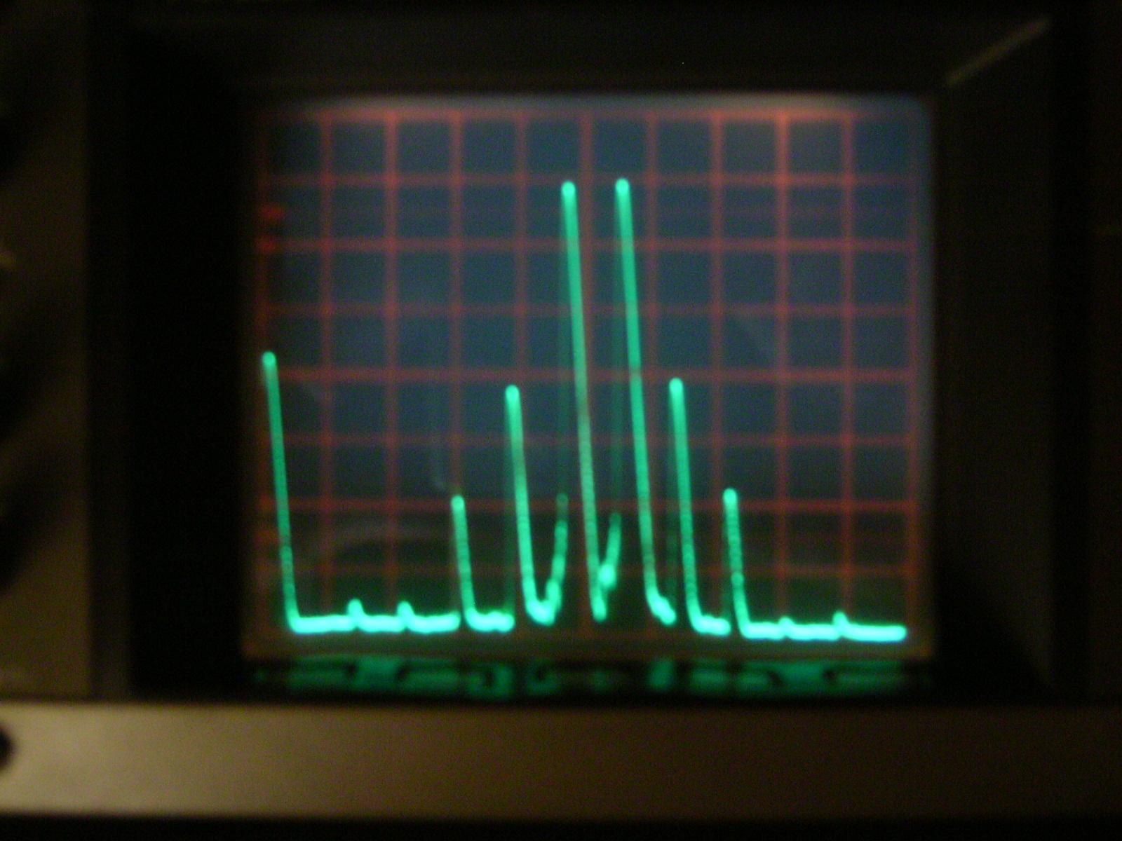
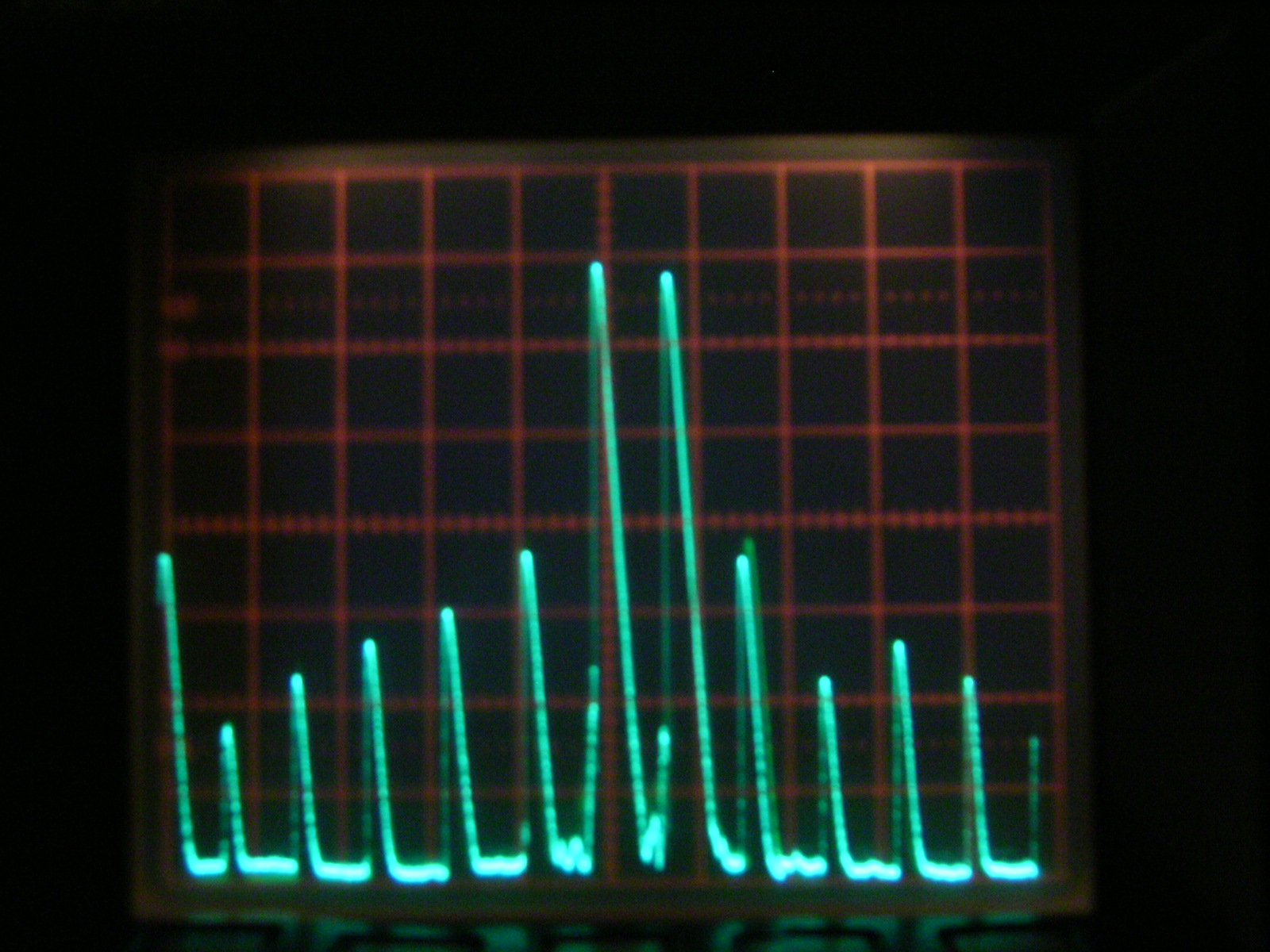
| 4 Mosfets Lin Ampl IMD Spectrum | 4 Transistors Lin Ampl IMD Spectrum |
 |
 |
|
Above is our 2x IRF510 + 2x IRF510
unit under RF 2 tone test: Gen1 at 14.150 Mhz Gen2 at 14.200 Mhz combined at the input for a PEP Output Power of 10 W measured with PEP Wattmeter closed to 50 Ohm dummy Load. V=28V A=1.520 (at 10 W PEP out) Efficiency= 23%. Vertical division 10 dB, horizontal division 50 Khz. We can see 3rd (-30 dB) and 5th IMD order (-50dB) and barely 7, 9th well attenuated. |
Above is our 2x 2SC2166 + 2x 2SC1969 under RF 2 tone test: Gen1 at 14.150 Mhz Gen2 at 14.200 Mhz combined at the input for a PEP Output Power of 10 W measured with PEP Wattmeter closed to 50 Ohm dummy Load. V=13.8V A=2.4 (at 10 W PEP out) Efficiency= 30%. Vertical division 10 dB, horizontal division 50 Khz. We can see a slightly better 3rd IMD (-32dB) but 5th (-40dB) IMD 7, 9, 11th order are much higher. |
FT1000MP Mark-V (TX finals 30V. very fine rugged Philips Mosfets)
-->click here for finals and IMD pictures class AB 200W, and class A bias at max 75W PEP,
from Yaesu brochure TX details)
FT1000MP Mark-V FIELD (TX finals 13.8V, high dissipation, 2SC2879 transistors)
-->click here for finals and IMD pictures class AB 100W, and class A bias at max 25W PEP,
from Yaesu brochure TX details)
FTDX9000 uses 50V STMicroelectronics RF Mosfets SD2931, see Yaesu brochure
(in JA7UDE web site, see IMD PHOTO AT 75 Watts Class A and 200 W class AB)
click here for:
----> Motorola Application Note AN790 link about "Thermal rating of RF power Transistors"

IC-7800 ICOM brochure (link to AB4OJ/VA7OJ web site) and schematic package. We see
that TX RF Power finals are a push-pull of modern ST  SD2931 rugged Mosfets at 48 V.
The pre-final is a single ST  SD2918. There are also two more single Mosfet stages at the low
level amplification input chain, ST  PD55003 driven by a Mitsubishi RD01MUS1, all mosfets.

See also in AB4OJ/VA7OJ A. Farson Icom pages my contribute (click on link below):
The RF Power Devices in the IC-7800 Transmitter

See also AB4OJ/VA7OJ YAESU QUADRA Mosfet linear amplifier (with MRF150 devices) page
MOSFETs LINEAR AMPL COMPONENT LIST:
C1,C2,C12,C13= 0,1 microFarad, 100 V.,5mm.,  metallised polyester
                   rectangular (ie type Arcotronics,  RS (Italy)-115988)
C5,C6= 0,22 microFarad, 100 V., 5mm.  (ie.  RS (italy)-116004)
C10,C18= 10 microFarad, 63 V., vertical electrolitic.
C3,C14,C7,C16,C9,C11,C19,C20= 0,1 microFarad, 63 V., 5mm., multilayer
                   (solder leads, when ground side, also in top components pcb side)
C4,C15,C8,C17= 0,01 microFarad, 63 V., 5 mm., multilayer
                   (solder leads, when ground side, also in top components side)
C29= 100 picoFarad, silver mica, 500 V. (CM05)
R1,R2=  10 Ohm, 1/4 Watt.
R3,R4,R7,R8,R15,R16=  100 Ohm, 1/4 W.
R5,R6=  3,9 KOhm, 1/4 W.
R9,R10=  180 Ohm, 1/4 W.
R11,R12,R13,R14=  4,7 Ohm, 1/2 W.
R17,R18=  2,2 KOhm, 1/4 W.
L1,L2= 1,5 microHenry (molded inductances ie. Siemens type)
RF-Chokes:
RFC1,RFC2= VK200
Ferrite-beads:
FB1,FB2= FB43-801 (Amidon)
RF Transformers data:
T1= 6 Amidon FT37-43 (permeab. 850) Amidon, 3 each leg
    Primary: 2 turns copper wire teflon insulated AWG 20 (TEF-20)
    Secondary: 3 turns copper wire teflon insulated AWG 20   "
T2= 6 Amidon FT37-43, 3 for each leg
    Primary: 3 turns copper wire teflon insulated AWG 20 (TEF-20)
    Secondary: 2 turns copper wire teflon insulated AWG 20  "
T3= 6 Amidon FT50-43, 3 for each leg
    Primary: 2 turns copper wire teflon insulated AWG 16 (TEF-16)
    Secondary: 3 turns copper wire teflon insulated AWG 16  "
T4= 1 Amidon FT50-43, n. 8 bifilar turns enameled wire, 0.5 mm. diameter

T5= 2 Amidon FT50-43, paired, n. 8  bifilar turns enameled wire, 0.8 mm. diameter

(See RF transformer details drawing)
Mosfets: Q1,Q2,Q3,Q4= IRF510 (IR International Rectifier or others)
BIAS REGULATOR COMPONENT LIST:
C21,C22,C23,C24,C25,C27,C28= 0,1 microFarad, 63 V., multilayer, 5mm.,
(solder the ground side lead also in the top component side of pcb)
C26= 1.000 picoFarad, multilayer, 5 mm.
R19= 100 KOhm, 1/4 W.
R20=  47 KOhm, 1/4 W.
R21=   4,7 KOhm, 1/4 W.
R22,R26= 10 KOhm, 1/4 W.
R23= 1 KOhm, 1/4 W.
R24= 10 Ohm, 1/4 W.
R25= 2 KOhm, 1%, 1/4 W.
R27= 8,2 KOhm, 1/4 W.
R31= Thermistor, 10 KOhm a 25°, 2,5 KOhm a 75°
Multiturn Trimmer:
R28= 10 KOhm, multiturn, vertical regulation (es. Spectrol, Bourns)
R29,R30= 10 KOhm, multiturn, vertical regulation    "       "
Impedances:
L3,L4= 150 microHenry (ie. Siemens type)
L5= 22 microHenry         "                   "
Active components:
Q5= 2N2222A
Q6= 2N2907A
U1= LM723CH (metalic can H or CH suffix by National, click for PDF file DATA)
Bibliography and notes (by IK4AUY):
1)  I Mosfet a RF di potenza sono stati variamente denominati dai vari
    costruttori ad es. VMOS (vertical MOS perche' la corrente scorre
    verticalmente nella geometria interna del chip), TMOS, DMOS  e tra
    i primi piu' noti produttori ricordiamo Siliconix (la serie DV
    specificata sino alle VHF, poi questo ramo e' stato ceduto
    ad altra azienda, e la serie VN, piu' simili ai ns. "commutatori
    veloci", ma gia' specificato per usi a RF) di cui citiamo ED OXNER,
    KB6QJ, che gia' nel n. 5/'79 di QST presento' un amplificatore lineare con
    VMOS); Motorola, la serie MRF1xx, ben documentata (in precedenza down load
    data sheet in http://mot2.mot-sps.com/rf/) in particolare da Helge Granberg,
    K7ES/OH2ZE, radioamatore ed ingegnere capo Motorola, ora vedi M/A-COM
    e per Philips, la serie BLFxxx (BLF147 sono i finali nel FT-1000MP-Mark V)
    Si veda:
    - VHF Communications 1/1982, Martin M., DJ7VY, A wide band driver
      for the shortwave bands, pag. 13-18, che utilizza un solo VN88 o VN89
      della Siliconix per il livello di P. out di 4 W pep.
    - QST (Arrl) 12/1982, Helge Granberg (Motorola staff), Mosfet RF Power:
      An Update, pag. 13-16, parte 1, e QST 1/1983 parte 2 in cui e'
      descritto un lineare da un kw costituito da un insieme di unita'
      con coppie di MRF150 in push pull, da 2-30 Mhz., alimentati con 50 V.
      Una configurazione similare e' stata successivamente sviluppata dalla
      Kenwood nel transceiver TS950SDX.
    - QST, 3/1983, Doug DeMaw, W1FB, Go Class B or C with Power MOSFETs,
      pag. 25-29, con un esempio di due MRF138 in push pull a 28V, pero'
      in questo esempio sono polarizzati per classe B o C, per uso solo in CW,
      non testati per intermodulazione, comunque questa famiglia di Mosfet
      e' specificata con buone caratteristiche di intermodulazione se in
      classe AB1 o meglio in classe A.
    - Ham Radio, 1/1984, DL4VJ e W7PUA, power FETs: trend for VHF amplifiers,
      pag. 12 e segg. sulla serie DV, fino a 100 W. a 144 Mhz.
    - QST, 2/1994, Gary Breed K9AY, AN Easy-to- Build 25 Watt MF/HF Amplifier,
      pag. 31-34, che utilizza un modulo con due JFET di potenza integrati
      in push pull, a 28 V. della MicroWave Technology, di non agevole
      reperibilita'.
    Alcuni apparati radioamatoriali che impiegano MOSFETS in push pull:
    FT920 A 13,8 V., IC 736, IC775, FT1000MP-MARK V a 28V, TS950SDX a 48V e
    IC-7800 a 48V.
    Inoltre Amplificatori Lineari HF che impiegano mosfet (MRF150): Yaesu QUADRA,
    ICOM PW1.
2)  Si veda Helge Granberg "Measuring the intermodulation distortion of
    linear amplifiers, EB38, reperibile in allegato al RF device data,
    vol. II, MOTOROLA. Inoltre: - Ham Radio, 4/1988, Marv Gonsior, W6FR,
    More operational notes on the TS-930S, che impiega transistor a 28 V.
    e spiega, riprendendo Helge Granberg, la linearita' in SSB.
    Assolutamente da non perdere: McGraw-Hill, William Sabin (W0IYH),
    Edgar Schoenike, Single Sideband System and Circuits, second edition,
    1995, (e' nel catalogo RS Components SPA-(MI)), scritto da ingegneri della
    Rockwell-COLLINS, in particolare il capitolo 12, Solid state power
    amplifier, ed il capitolo 13 Ultra-lowdistorsion power amplifier, in
    riferimento specifico alla linearita' dei Mosfets. Questo libro ha ora una
    nuova edizione, recensita in QST, 5/1999, Noble Publishing Corp., HF Radio
    System & Circuits, ed. 1998, stessi autori (http://www.noblepub.com/)
    ed e' anche nel catalogo della ARRL.
    In sintesi l'IMD, con il test a due toni (in questo caso generati dalla
    combinazione di due segnali a RF distanti fra di loro tipicamente
    circa due khz, ed anche 20 Khz per vedere se ci sono differenze) puo'
    essere espressa, in relazione al prodotto di 3ø, 5ø, 7ø ... ordine
    secondo due convenzioni.
    Si premette che se F1=14,100 Mhz, F2=14,120 Mhz, l'intermodulazione del 3ø
    ordine appare visibile in un analizzatore di spettro a 14,080 e 14,140
    Mhz, purche' lo strumento possieda la necessaria selettivita', il segnale
    venga accoppiato allo strumento con attenuazione ad un livello appropriato
    che non provochi la compressione dello strumento stesso, inoltre i due
    segnali fondamentali siano visualizzati sull' analizzatore di spettro al
    medesimo livello, a prescindere da come sia letta la P out dell'
    amplificatore, in Watt continui/medi oppure P.e.P. e solo se a parita' di
    queste condizioni e' corretto effettuare letture di confronto tra IMD di
    questo amplificatore a frequenze diverse oppure in relazione ad altri
    amplificatori di diverso progetto.
    Gli standard di misura della IMD sono:
    a) in dB di attenuazione in riferimento ad ognuno dei due eguali toni
       desiderati, secondo lo standard militare (Mil-std-1131 Version A -
       test method 2204B). Questa e' la procedura da noi adottata nel
       rilevare i dati di IMD nella tabella B e C. (-dBc, we used this one)
    b) in dB di attenuazione in relazione alla potenza di picco dell'
    amplificatore, p.e.p., nella prova a due toni eguali, secondo lo standard
    commerciale EIA, seguito dalla maggior parte dei costruttori di apparati
    radioamatoriali e pure dal laboratorio della ARRL nelle loro prove degli
    apparati nuovi (fonte Test procedures manual - ARRL).
    Seguendo quest'ultimo metodo si ha un valore di IMD migliore sulla carta
    di 6 dB poiche' riferito al livello p.e.p. dei due toni che e' appunto
    6 dB maggiore rispetto alla potenza di ogni singolo tono, (es. -30 dB. nel
    caso a) equivale a -36 dB nel caso b), pertanto anche i ns. dati nelle
    tabelle B-C devono essere aumentati di 6 dB in valore assoluto per un
    corretto confronto). In pratica la lettura diretta nell'analizzatore
    di sprettro viene effettuata, con questo standard, facendo scorrere in
    verticale i due eguali toni ad un livello dello schermo posizionato 6 dB
    al di sotto dello zero di riferimento, anziche' sullo zero come nel caso
    a).
    I livelli di P. out sono stati letti, nel nostro caso, con BIRD mod. 43
    che e' un wattmetro che legge una potenza continua o media nel caso siano
    presenti piu' toni, ma non p.e.p. pertanto fare attenzione se utilizzate
    un wattmetro nella posizione p.e.p.
    BIRD precisa infatti che, in presenza di due toni, ad es. 100 watt
    p.e.p. vengono letti dal mod. 43 come 40,5 w. (che approssima l' average
    power pari alla meta' del p.e.p. ovvero 50 w.; i modelli Bird della serie
    4380/4391, digitali, riescono a leggere anche la potenza di ogni singolo
    tono, ovvero 25 w., cioe' esattamente 6 dB in meno rispetto al valore
    p.e.p.)  (Watt's new from BIRD, vol. 4, nø 2. e tabella riassuntiva
    di confronto tra letture nei modi diversi di emissione riportata nel
    catalogo generale Bird). Pertanto per realizzare la summenzionata parita'
    di condizioni nelle prove di IMD, per un corretto confronto, occorre
    misurare livelli di P out equivalenti.
3)  Il piu' recente e completo articolo sui Mosfet da commutazione per uso
    RF e' di Mike Kossor, WA2EBY, in QST, 3/1999 e 4/1999, A broadband HF
    Amplifier Using Low-Cost Power MOSFETS che similarmente alla nostra
    esperienza impiega un push pull di 2 IRF510 a 28 V., ma non risolve
    ancora il problema della linearizzazione della relazione guadagno -
    frequenza, il punto di lavoro e' in classe C , e per conseguenza
    non viene presentata alcuna prova sulla intermodulazione a due toni.
    In precedenti articoli su Mosfet a basso costo, in quest'ultimo e'
    riportata ulteriore bibliografia, la relazione guadagno frequenza era
    assai piu' limitata.
4)  Si veda di Helge Granberg la nota applicativa Motorola AN860, "Power
    mosfets versus bipolar transistors", ed ancora AR165S "RF power Mosfets"
    e l'ottimo libro "Radio Frequency Transistors: principles and practical
    applications" di Norm Dye - Helge Granberg, ed. 1993, edito da
    Butterworth-Heinemann (e' nel catalogo della RS Components SpA (MI) e
    tratta anche dei Mosfets a RF con riferimenti specifici alla configurazione
    push-pull).
5)  Il "data sheet"  relativo all' IRF510 e' reperibile nel databook
    HARRIS  "POWER MOSFETS", IR International Rectifier (down load il file
    .pdf al sito http://www.irf.com/product-info/datasheets/data/irf510.pdf
6)  Soluzione gia' presentata in precedenza nel caso di push-pull di
    transistor nelle note applicative di Helge Granberg della Motorola,
    ad es. in AN762, reperibili in allegato al libro "RF Device data -
    vol. II" ed ora anche in Motorola RF Application Report.
7)  Da Helge Granberg in QST 12/1982, vedi nota 1), e dal suo libro
    con Norm Dye in nota 4), paragrafo biasing of mosfets pagg. 64-68.
8)  Si veda Norm Dye - Helge Granberg, libro in nota 4), capitolo 12, par.
    negative feedback.
    Nella coppia del primo stadio, al posto dei due IRF510, sono stati da
    noi testati inizialmente anche due VN88AF Siliconix con buoni risultati,
    tuttavia considerando che la piedinatura e' diversa, il prezzo e'
    superiore, ed i risultati non si discostano di molto, abbiamo scelto
    di non utilizzarli.
9)  Noi usiamo un bromografo autocostruito, pubblicato sul bollettino
    della Sezione ARI di Bologna in cinque numeri, dal 1992 al 1993, da
    I4FAF. Si veda anche in R.R. 10/98, IK5NTH, pagg. 26-28.
    La vetronite a doppia faccia di rame pre - sensibilizzata e' reperibile
    presso Ham Center SRL, Via Cartiera 69, Borgonuovo di Pontecchio Marconi
    (BO) - 40044,I4PZP, che ringraziamo per averci fornito anche ampia gamma di
    ferriti Amidon per la selezione dei mix e dimensioni piu' idonee per i
    trasformatori RF.
10) Se proprio non riuscite a reperire cavo isolato in teflon:
    RF PARTS (California) http://www.rfparts.com/11) L'idea e' stata tratta dal manuale di servizio TEN-TEC - PARAGON,
    anche se in quel caso l'amplificatore era a transistor e non a Mosfet.
12) Ad esempio Advanced Power Technology offre Mosfet a RF, in TO-247
    serie ARF4xx, in particolare ARF449A e ARF449B, tensione max 150 V.,
    di lavoro sugli 60 - max 85 V., caratterizzati fino ad un massimo di 120 Mhz,
    e la lettera A e B indica che si tratta di una coppia con piedinatura
    differente, ma simmetrica, per un lay out perfettamente simmetrico
    nelle configurazioni push-pull. Si veda nota applicativa di Richard Frey,
    K4XU, "A 300W Mosfet Linear Amplifier for 50 Mhz" reperibile al sito
    http://www.advancedpower.com/, in cui e' possibile il down load anche
    dei data sheet. Questo progetto sta per essere presentato in QEX-ARRL,
    Maggio-Giugno 1999. Nota (16.07.2003): la ns. esperienza con alcuni mosfet APT
    come amplificatori Push-Pull Broadband HF per radioamatori  NON e'
    stata subito positiva  a meno di alimentarli a tensioni max 60 - 80 Volts.
    Idonei allo scopo, tra i vari, gli MRF150 M/A-COM a 48 Volts, di prezzo piu' elevato.