 |
A High-Level Accessory Front End for the HF Amateur Bands
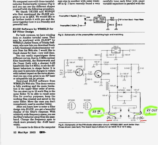
QEX MARCH –APRIL 2003 PAGE 52 ERRATA CORRIGE
|
|
Until now I have found only one mistake in QEX March-April 2003 page 52, Fig. 6, schematic of the PIN-diode attenuator circuit in which the by-pass relay must be as follow (our pc board template is OK): RF In goes to the common and RF Out goes to the other common.
100nF input capacitor goes to K11A terminal, the output 100 nF capacitor goes to K11B terminal. Of course the relay position indicated is at normaly close OFF position (NOT exited), so RF is bypassed by the short and the attenuator circuit is kept outside the RF path.
One more odd thing:
I have discovered a very powerful tool to play with receiver gain, noise, IP3, MDS, per stage and cumulatives data to simulate with a complete receiver system without getting tired about long calculations.
Try this professional-nice and available for free software by AGILENT: Version 2.5.1 AppCAD
Download file name: setup251.exe
Download file size: 12.2 MBhttp://www.agilent.com/view/appcad
Choose the menu function "Noise Calc". And enjoy it.
I have some more info, and dBm to dBmicroV easy conversion relations, in
my web site
at
http://www.qsl.net/ik4auy/article_5.htm (under Measures & simulations an article in Italian which is under future
publication in our ARI magazine, but the relations are easy to read).
Best Regards. Sergio Cartoceti, IK4AUY
|
Down load here May/June 2003 QEX .pdf file "Letter to
Editor" a link to Neoamateur.org download page |